What in Electronics?
PCB Design
-



 17:13
10
17:13
10
- 1 Learn PCB Designing Just in 15 Minutes! EasyEDA + JLCPCB Complete Tutorial 2023 17:13
- 2 Top Fifteen Mistakes People Make When Designing Prototype PCBs 12:26
- 3 6 Horribly Common PCB Design Mistakes 10:40
- 4 PCB making, PCB prototyping quickly and easy – STEP by STEP 10:16
- 5 Beginners guide to PCB design with EasyEda Part 1 11:16
-




 11:10
10
11:10
10
- 1 An Intro to KiCad – Part 1: How PCBs Are Made | DigiKey 11:10
- 2 An Intro to KiCad – Part 2: Create a Schematic Symbol | DigiKey 11:18
- 3 An Intro to KiCad – Part 3: Schematic Capture | DigiKey 15:50
- 4 An Intro to KiCad – Part 4: Create a Footprint | DigiKey 20:16
- 5 An Intro to KiCad – Part 5: Associate Footprints and Generate Netlist | DigiKey 15:37
-



 9:12
18
9:12
18
- 1 Build a KiCad Project Schematic | Part 1 9:12
- 2 KiCad Custom Parts | Part 2 10:55
- 3 KiCad Choosing Parts | Part 3 11:23
- 4 KiCAD Custom Footprint | Part 4 9:51
- 5 KiCAD Project PCB Prep | Part 5 | Setting Up Your PCB for Manufacturing 4:09
-


 4:50
23
4:50
23
- 1 #1 How To Use New Kicad 7.0 – Introduction | #PCBCupid 4:50
- 2 #2 How To Use New Kicad 7.0 User Interface | #PCBCupid 6:30
- 3 #3 How To Design A Circuit Using KiCad 7.0 Schematic Editor | #PCBCupid 7:46
- 4 #4 How To Prettify Your Schematic with Kicad 7.0 | #PCBCupid 7:06
- 5 #5 How To Perform ERC and What Is Footprint In KiCad 7.0 | #PCBCupid 9:35
-


 2:24
14
2:24
14
- 1 001 EasyEDA Introduction 2:24
- 2 002 How to Create the Project 6:23
- 3 003 Teamwork at EasyEDA 2:52
- 4 004 Version Control 1:42
- 5 005 Create Schematic Symbol 3:48
-



 1:34:41
7
1:34:41
7
- 1 Altium Designer 22 Tutorial – Quick & Easy | Step by Step 1:34:41
- 2 Altium Tutorial for Beginners: How to do Schematic & PCB Layout 17:46
- 3 Altium Designer – Create BOM & Library from Supplier’s Data 6:31
- 4 Altium Designer – 3D model of your PCB – it’s really easy 9:31
- 5 Altium Designer – How to Create Assembly Drawing Layers 13:06
-


 4:30
7
4:30
7
- 1 KiCad 9.0 – Getting Started Part 1: Intro & Download | DigiKey 4:30
- 2 KiCad 9.0 – Getting Started Part 2: Schematic Layout | DigiKey 9:51
- 3 KiCad 9.0 – Getting started Part 3: Create a Custom Schematic Symbol | DigiKey 5:56
- 4 KiCad 9.0 – Getting Started Part 4- Finishing the Schematic – DigiKey 5:49
- 5 KiCad 9.0 – Getting Started Part 5 – Assigning & Creating Custom Footprints | DigiKey 9:26
-



 2:04
33
2:04
33
- 1 Easy EDA Complete Course in UrduHindi | Easyeda Tutorials | PCB Design Course in Hindi / Urdu 2:04
- 2 Easyeda Onlne PCB Design Software Introduction and tour | Circuit Designing software complete course 12:00
- 3 What is schematic How to read and follow schematic diagram Easyeda online | easyeda PCB design 8:46
- 4 How to use EasyEDA online Components Library | easyeda components library | easyeda online PCB 11:32
- 5 How to use easyeda online Bus tool, Bus Entry, Netlabel tools in schematic Easyeda in hindiurdu 11:23
-


 15:39
36
15:39
36
- 1 How to make a PCB – Ep 1 – Install Kicad and Make Schmatic 15:39
- 2 How to make a PCB – Ep 2 – PCB layout design 21:35
- 3 KiCad Tutorial – Create a Schematic Symbol in Kicad 14:48
- 4 KiCad Tutorial – How to create your own Footprint in KiCad 16:47
- 5 KiCad Tutorial – How to Import Footprint Step file 7:24
-


 8:39
9
8:39
9
- 1 KiCAD 9 tutorial course [01] – Introduction 8:39
- 2 KiCAD 9 tutorial course [02] – Simple project 44:37
- 3 KiCAD 9 tutorial course [03] – Schematic editor 34:22
- 4 KiCAD 9 tutorial course [04] – PCB editor 54:17
- 5 KiCAD 9 tutorial course [05] – Symbol editor 14:38
-


 4:21
41
4:21
41
- 1 1.1 Feature Overview 4:21
- 2 1.2 Software Installation 2:43
- 3 1.3 Software Settings 4:58
- 4 1.4 Create Project 1:11
- 5 1.5 Project Management 2:38
-


 23:37
314
23:37
314
- 1 Altium Designer Quick-Start Tutorial with Phil Salmony from Phil’s Lab 23:37
- 2 Top 5 Beginner PCB Design Mistakes (and how to fix them) 12:52
- 3 Master the Art of Component Choice 13:58
- 4 I2C and SPI on a PCB Explained! 15:34
- 5 How to Start a Project in Altium Designer | Module 1 8:18
-


 2:28
14
2:28
14
- 1 Introduction to PCB Design with EasyEDA Online Course 2:28
- 2 Introduction to PCB Design with EasyEDA a Free And Online Tool 16:43
- 3 How To Create Schematic with easyEDA 20:29
- 4 How to create PCB Layout with EasyEDA 16:44
- 5 How To Create Transistorized PCB Project with EasyEDA 15:46
-




 19:52
13
19:52
13
- 1 KiCAD Tutorial #1: Introduction and UI 19:52
- 2 KiCAD Tutorial #2: Organising the Schematic and Top Sheet 21:20
- 3 KiCAD Tutorial #3: Creating Schematic 28:54
- 4 KiCAD Tutorial #4: Easy Guide to Net Classes 41:20
- 5 KiCAD Tutorial #5: PCB Design Workflow 21:17
-
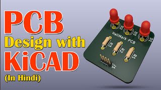


 26:28
21
26:28
21
- 1 How to design your own PCB in KiCAD | For beginner | Printed Circuit Board Design in Hindi 26:28
- 2 How to Download and Install KiCAD | PCB Design with KiCAD in Hindi 9:30
- 3 KiCad PCB Design | 3D Model | Circuit Design & Development 0:20
- 4 KiCAD PCB Design Course for Beginners in Hindi 2022 | Level up your PCB Design Skill with KiCAD 2:21
- 5 How to design your own PCB in KiCAD | For beginner | IR Sensor Design in Hindi 19:38
-


 24:28
10
24:28
10
- 1 Master EasyEDA | Project 01 | Upskill your PCB designing in 2024 | EasyEDA tutorials | Ampnics 24:28
- 2 Master EasyEDA | Project 02 | Upskill your PCB designing in 2024 | EasyEDA tutorials | Ampnics 18:20
- 3 Master EasyEDA | Project 03 | Upskill your PCB designing in 2024 | EasyEDA tutorials | Ampnics 14:25
- 4 Master EasyEDA | Project 04 | Upskill your PCB designing in 2024 | EasyEDA tutorials | Ampnics 13:57
- 5 Master EasyEDA | Project 05 | Upskill your PCB designing in 2024 | EasyEDA tutorials | Ampnics 13:40
-




 2:36
171
2:36
171
- 1 Quick Tips [Schematic 1] : Set Up The Common Library 2:36
- 2 Quick Tips [Schematic 2] : DRC check 3:03
- 3 Quick Tips [Schematic 3] : Find Similar 1:18
- 4 Quick Tips [Schematic 4] : Drawing Size 4:02
- 5 Quick Tips [Schematic 5] : Find & Replace 2:23
-




 1:02
11
1:02
11
- 1 EasyEDA V3 New Features Series | Projects & Libraries Recycle Bin 1:02
- 2 EasyEDA V3 New Features Series | Project & Document Historical Records 1:01
- 3 EasyEDA V3 New Features Series | Dark Mode & Interface Themes 1:04
- 4 EasyEDA V3 New Features Series | Version Control & Branch Management 3:12
- 5 EasyEDA V3 New Features Series | Component Placement History Tracking 1:55